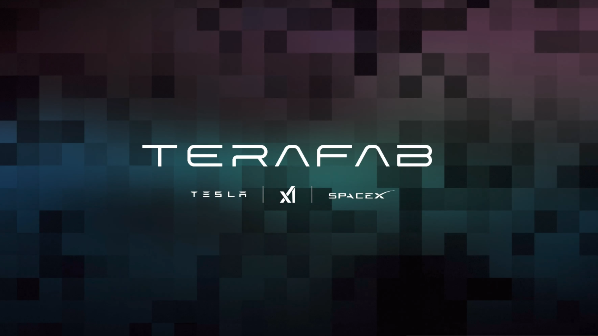
Elon Musk spills more beans about TeraFab.

www.tomshardware.com
Elon Musk says his TeraFab facilities will use Intel's 14A process technology to make AI chips — SpaceX will be responsible for high-volume chip manufacturing in likely Intel tech licensing deal
Elon Musk on Wednesday said that TeraFab plans to use Intel's 14A fabrication technology when it has its own production capacity later this decade and when the manufacturing process matures. He also revealed that Tesla will be responsible for building and operating a pilot production line, whereas SpaceX will be responsible for high-volume manufacturing of chips.
TeraFab to use Intel 14A
"We plan to use Intel's 14A process, which is state-of-the-art and in fact not yet totally complete," Elon Musk, chief executive of Tesla, said during Tesla's earning's call with analysts and investors. "By the time TeraFab scales up, 14A will be probably fairly mature or ready for prime time. 14A seems like the right move and we have a great relationship with Intel, a lot of respect for the CEO, the CTO, and the new team there."
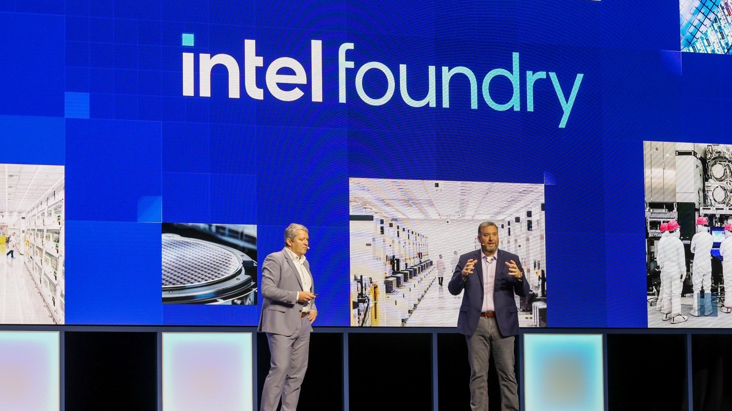
Based on the comments made by Musk, he wants to use Intel's 14A manufacturing technology at TeraFab, which likely means licensing the fabrication node from Intel and integrating it at a fab operated by TeraFab. Meanwhile, Musk has never mentioned licensing per se, which means that while Intel is expected to participate in TeraFab as a partner, actual details of its role have yet to be defined.
As for Tesla and SpaceX, the division of responsibilities is straightforward: Tesla handles the research fab, while SpaceX builds and operates a high-volume manufacturing facility.
Tesla handles R&D, SpaceX handles manufacturing
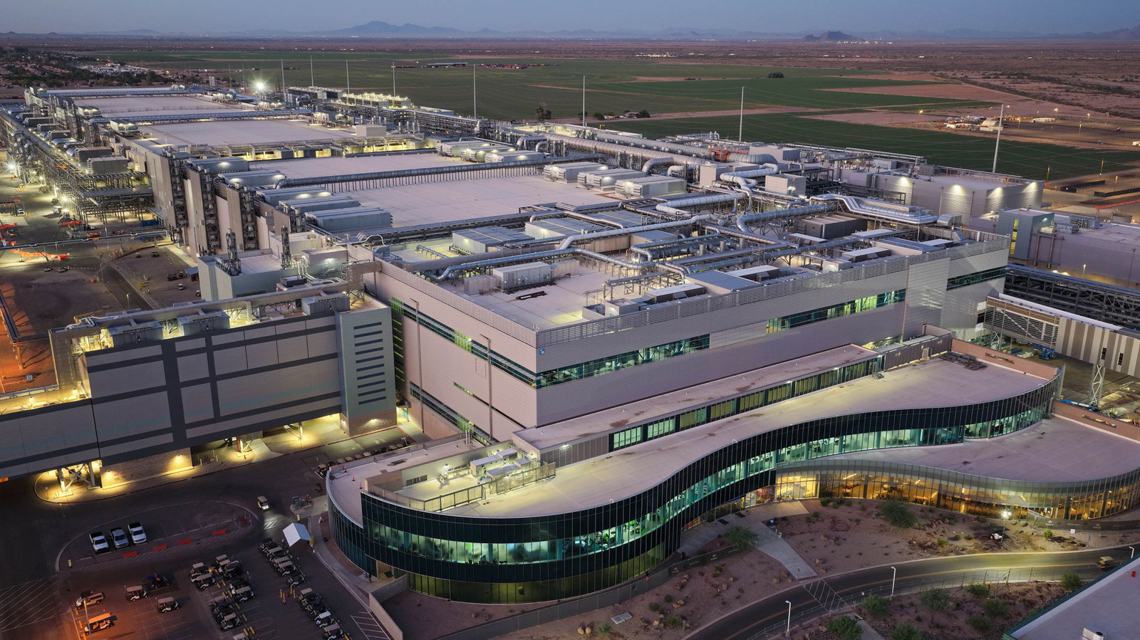
In the short term, Tesla intends to construct a semiconductor R&D facility at its Texas campus, with an estimated cost of around $3 billion. This site will be a small pilot line capable of processing a few thousand wafers per month, and its purpose will be to experiment with new ideas in semiconductor manufacturing as well as validate whether these ideas can be realized in a production-like environment. From what we can tell, 14A will barely have anything to do with the pilot line in Texas.
"In the near term, Tesla plans to build a research fab at its Gigafactory Texas campus," Musk said. "This is something we expect to be a $3 billion initiative and support a few thousand wafers per month. "It is really intended to try out ideas […] for improving the fundamental technology of how chips are made, some of new physics we would like to test out. We also want to test out the ability to see if something is working in production [environment]. You need kind of like a few thousand wafer starts a month to make sure that a production process is sound."
For scaling beyond the pilot phase, SpaceX is expected to build an actual high-volume manufacturing facility. However, coordination between Tesla and SpaceX introduces many challenges, as any joint effort must be approved by both companies' boards and pass conflict-of-interest reviews, which will inevitably slow down the project.
"That is basically what we have figured out thus far is Tesla's doing the research fab, SpaceX doing the initial part of the large-scale TeraFab and then we got to figure out the rest," Musk said.
Licensing a process technology is one of the ways for TeraFab to get a fabrication node quickly (as it may take a decade to design a manufacturing tech from scratch), whereas for Intel, this could mean an influx of cash. Historically, chipmakers have licensed process technologies from others if they could not design their own node on time, or the parties wanted to create a virtual foundry with compelling capacity to compete with larger contract chipmakers.
For example, GlobalFoundries licensed Samsung's 14nm-class process technologies in 2014 – 2015 after it failed to complete development of its own 14nm XM production node. While there were rumors that GlobalFoundries produced some of Samsung's Exynos processors at its fab in New York, the first clearly attributable, high-volume GF-built 14nm products — AMD's
Radeon RX 400-series 'Polaris' GPUs only showed up in 2016. This incited rumors about GF's inability to integrate the node and maximize yields.
Rapidus is a more recent example, as it has licensed IBM's 2nm technology for its fabs.
It remains to be seen whether it is possible to license Intel's 1.4nm-class process technology and then port process recipes, tune tools, and maximize yields at a TeraFab facility. After all, modern process technologies are dramatically more complex than those from a decade ago.